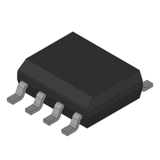
Components for hardware design: Selection of diodes, transistors and MOS tubes
The cornerstone of hardware design: components
In today's era of rapid technological development, hardware design, as the core link in the field of electronic engineering, supports the birth of countless smart devices and innovative products. From the smartphones and laptops we use in daily life to the automation equipment in industrial production and precision instruments in the medical field, all are masterpieces of hardware design. In the huge system of hardware design, the selection of components is the top priority. It is like the cornerstone of a building, which directly determines the performance, stability and cost of the hardware system.
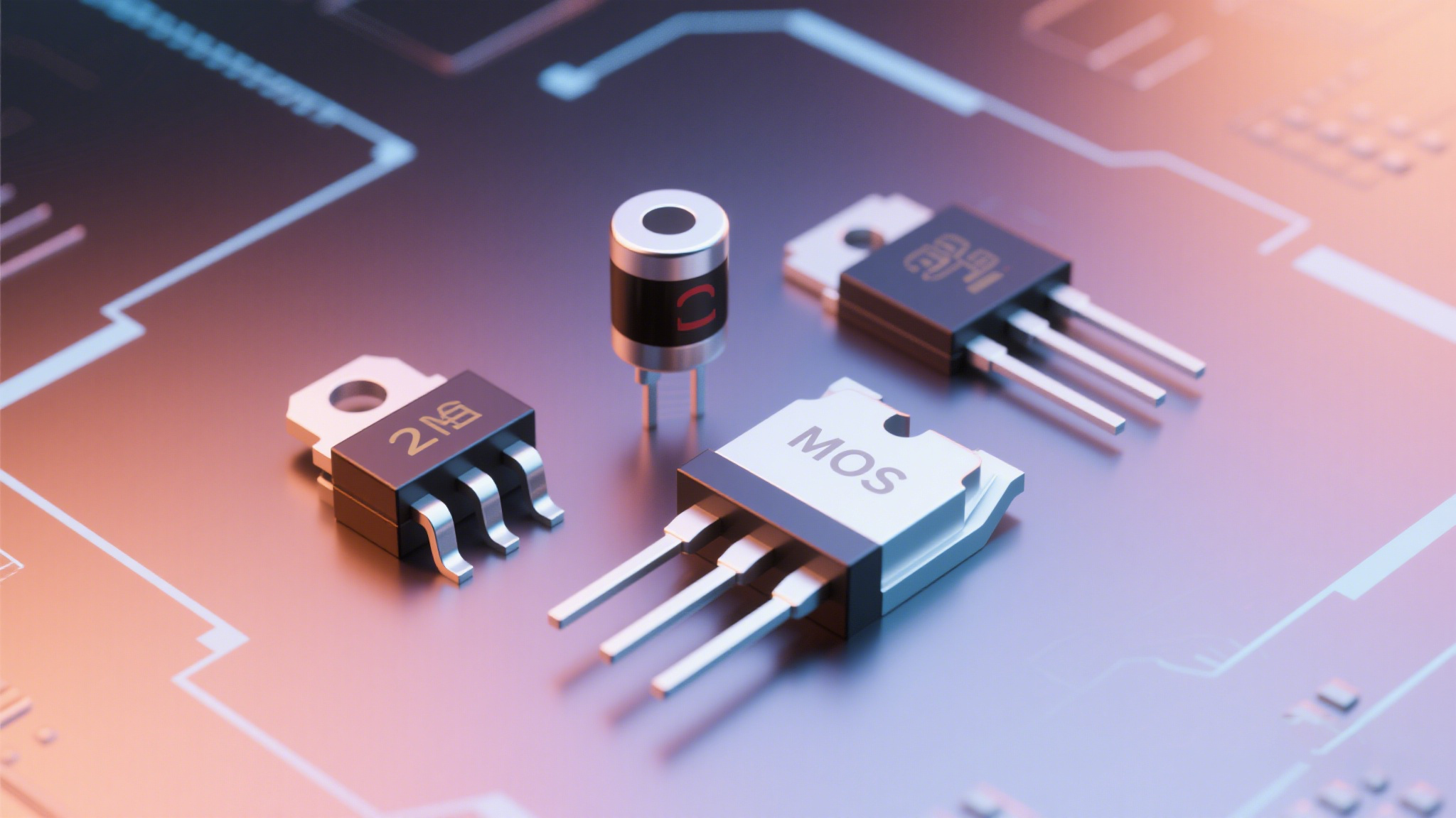
Diodes, triodes and MOS tubes, as the most basic and key components in hardware design, are small in size but contain huge energy and play an irreplaceable role in various circuits. Their unique physical properties and electrical properties provide rich possibilities for circuit design, enabling engineers to build circuit systems with different functions and complex and exquisite functions. Next, let us explore the world of these three components in depth and unveil their mystery in hardware design.
Diode: Selection points and application scenarios
Working principle of diode
Diode is a semiconductor device based on PN junction, and its core characteristic is unidirectional conductivity. Simply put, the PN junction is formed by the close combination of P-type semiconductor and N-type semiconductor. In P-type semiconductor, holes are the main carriers and show positive charge characteristics; N-type semiconductors use electrons as the main carriers and carry negative charges. When P-type and N-type semiconductors are combined, a special area is formed at their interface, namely the space charge area, also known as the PN junction.
In the absence of external voltage, the carriers on both sides of the PN junction will diffuse due to the concentration difference, forming a built-in electric field. This built-in electric field will prevent the further diffusion of carriers, so that the PN junction is in a dynamic equilibrium state. When a forward bias voltage is applied to both ends of the diode, that is, the P region is connected to the positive pole of the power supply and the N region is connected to the negative pole of the power supply, the external electric field is opposite to the built-in electric field, which weakens the blocking effect of the built-in electric field, allowing the holes in the P region and the electrons in the N region to pass through the PN junction smoothly, forming a forward current, and the diode is turned on. When a reverse bias voltage is applied, that is, the P region is connected to the negative pole of the power supply and the N region is connected to the positive pole of the power supply, the external electric field is in the same direction as the built-in electric field, which strengthens the blocking effect of the built-in electric field, and it is difficult for carriers to pass through the PN junction. There is only an extremely weak reverse saturation current, and the diode is cut off.
Key parameters for selection
◎ Maximum forward current: refers to the maximum average forward current that the diode can withstand when it works normally for a long time. It is closely related to the area of the PN junction, heat dissipation conditions, etc. In practical applications, if the forward current exceeds this value, the diode may be damaged due to overheating. For example, in some high-power power supply rectifier circuits, it is necessary to select a diode with a large maximum forward current to ensure that it can withstand the passage of large currents.
◎ Reverse breakdown voltage: This is the maximum reverse voltage that a diode can withstand. When the reverse voltage exceeds this value, the PN junction of the diode will be broken down, losing unidirectional conductivity, and may cause permanent damage. When designing a high-voltage circuit, it is necessary to ensure that the reverse breakdown voltage of the selected diode is much higher than the actual reverse voltage in the circuit to ensure safe and stable operation of the circuit.
◎ Switching speed: For diodes used in high-frequency switching circuits, switching speed is a key parameter. It is mainly measured by the reverse recovery time, that is, the time required for the diode to switch from the forward conduction state to the reverse cutoff state. Diodes with fast switching speeds can respond quickly to the rapid switching of high-frequency signals, reducing energy loss and signal distortion. In fields such as high-frequency communication circuits and switching power supplies, diodes with fast switching speeds are required.
◎ Forward voltage drop: The voltage drop across the diode when it is forward-conducting. The lower the forward voltage drop, the less power loss the diode has in the on state, and the higher the efficiency. In battery-powered devices with strict power consumption requirements, diodes with lower forward voltage drops are usually selected.
Application scenario analysis
◎ Rectifier circuit: This is one of the most common applications of diodes. In the process of converting AC power to DC power, the rectifier diode uses its unidirectional conductivity to process the positive and negative half cycles of AC power, so that the current always flows in one direction, thereby achieving the purpose of rectification. Common rectifier circuits include half-wave rectification, full-wave rectification and bridge rectification. In the half-wave rectification circuit, only half of the cycle of AC power is used, and the rectification efficiency is low; full-wave rectification and bridge rectification can make full use of the positive and negative half cycles of AC power, improving the rectification efficiency. When selecting a rectifier diode, it is necessary to comprehensively consider the maximum forward current, reverse breakdown voltage and reverse recovery time of the diode based on the input voltage, output current and power frequency of the circuit. For example, for a power rectifier circuit with a 220V AC input, a diode with a reverse breakdown voltage greater than 600V is usually selected; and for large current output occasions, it is necessary to ensure that the maximum forward current of the diode meets the requirements.
◎ Voltage regulator circuit: The voltage regulator diode is a special diode that can maintain voltage stability in the reverse breakdown state. When the input voltage fluctuates or the load changes, the voltage regulator diode adjusts the voltage by changing its own current, so that the output voltage remains within a relatively stable range. When designing a voltage regulator circuit, the key is to select a voltage regulator diode with a suitable voltage regulator value according to the required stable voltage value, and reasonably calculate the resistance value of the current limiting resistor to ensure that the voltage regulator diode works in a safe and reliable state. For example, for a circuit that needs to output a stable 5V voltage, it is necessary to select a voltage regulator diode with a voltage regulator value close to 5V.
◎ LED drive circuit: In the LED drive circuit, the diode mainly plays a role in protection and current control. Since LED is a current-type device, it has high requirements for current stability. The diode can prevent the reverse current from damaging the LED, and cooperate with other components to achieve precise control of the LED current to ensure the normal light emission and life of the LED. In this application scenario, it is necessary to select a diode with a suitable forward voltage drop and a maximum forward current that meets the requirements according to the operating current and voltage characteristics of the LED.
Transistor: Dual roles of amplification and switching
Structure and principle of transistor
Transistor, full name semiconductor transistor, also known as bipolar transistor, is an extremely important current-controlled semiconductor device. Its internal structure is mainly composed of three doped regions, namely emitter (Emitter, E), base (Base, B) and collector (Collector, C). According to the different combinations of semiconductor types in these three regions, transistors are mainly divided into NPN type and PNP type.
NPN type transistor is composed of two N-type semiconductors sandwiching a P-type semiconductor, the P-type semiconductor is used as the base region, and the N-type semiconductors on both sides are the collector and emitter respectively. The PNP type transistor is composed of two P-type semiconductors sandwiching an N-type semiconductor, the N-type semiconductor is used as the base region, and the P-type semiconductors on both sides are the emitter and collector respectively.
The core working principle of the transistor is based on the characteristics of the PN junction, which controls the large current (collector current IC) through a small current (base current IB). Taking the NPN transistor as an example, when a forward bias voltage (VBE) is added between the base and the emitter, and VBE is greater than the threshold voltage of the silicon tube (usually about 0.7V), the emitter junction is turned on, and a large number of electrons from the emitter are injected into the base region. Since the base region is very thin and the doping concentration is low, only a small part of the electrons will recombine with the holes in the base region to form the base current IB , while most of the electrons will drift to the collector under the action of the collector junction electric field to form the collector current IC . Moreover, there is a fixed proportional relationship between the collector current IC and the base current IB , that is, IC = β × IB , where β is the current amplification factor, which is generally between tens and hundreds. This means that a small change in the base current can cause a large change in the collector current, thereby realizing the signal amplification function. When the transistor works in the switching mode, it is mainly in the cut-off region and the saturation region. In the cut-off region, the base-emitter voltage VBE is less than the threshold voltage, the base current IB is approximately 0, and the collector current IC is also almost 0, and the transistor is equivalent to a switch disconnected. In the saturation region, the base current IB is large enough to make the collector current IC reach the maximum value. At this time, the collector-emitter voltage VCE of the transistor is very small, usually less than 0.3V, and the transistor is equivalent to a closed switch.
Selection considerations
◎ Current gain: that is, the β value, which reflects the transistor's ability to amplify current. Different application scenarios have different requirements for the β value. Generally speaking, in small signal amplifier circuits, it is necessary to select transistors with large and stable β values to obtain better amplification effects; in switching circuits, the requirements for β values are relatively low, but they still need to be guaranteed to be within a certain range to ensure that the transistor can be reliably turned on and off. For example, the common small signal amplifier transistor 2N3904, its β value is usually between 100-300.
◎ Maximum collector current: refers to the maximum current allowed to pass through the collector when the transistor can work normally. When selecting a transistor, it is necessary to ensure that the actual collector current in the circuit is less than this value, otherwise the transistor may be damaged due to overheating. For example, in a circuit that drives a high current load such as a relay, it is necessary to select a transistor with a suitable maximum collector current based on the pull-in current of the relay. For example, the maximum collector current of 2N2222 can reach 800mA. Power consumption: During the operation of the transistor, the collector current will generate heat on the collector junction, resulting in power consumption. Its power consumption PDcan be calculated by the formula PD=VCE × IC . When selecting a transistor, it is necessary to consider the power consumption based on the heat dissipation conditions of the circuit. For applications with high power consumption, it may be necessary to equip the transistor with a heat sink to ensure that its operating temperature is within the allowable range.
◎ Frequency characteristics: measured by the characteristic frequency fT , which indicates the frequency corresponding to when the current amplification factor β of the transistor drops to 1. In high-frequency circuits, transistors with a high enough fT should be selected to ensure that they can work properly without signal distortion or reduced amplification capability. For example, for RF circuits with operating frequencies of tens of MHz or even higher, high-frequency transistors 2SC3356 are often selected, and their fT can reach more than 2GHz.
Typical application cases
◎ Common-emitter amplifier: This is one of the most common amplifier circuits for transistors. In a common-emitter amplifier, the input signal is added between the base and the emitter, and the output signal is taken between the collector and the emitter. By reasonably setting the base bias resistor and the collector load resistor, the transistor can be operated in the amplification area, thereby achieving amplification of the input signal. This circuit has a high voltage amplification factor and power amplification factor, and is widely used in audio amplification, RF amplification and other fields. For example, in a simple audio amplifier, by adjusting the values of the base resistor RB and the collector resistor RC, the transistor can amplify the weak audio signal from the microphone to a level sufficient to drive the speaker to produce sound.
◎ Switching circuit: The transistor plays a vital role in the switching circuit. By controlling the level signal of the base, the on-off control of the high current load can be achieved. When the base input is high level, the transistor is saturated and turned on, and the load circuit is connected; when the base input is low level, the transistor is cut off and the load circuit is disconnected. In applications such as controlling the on and off of LEDs and the start and stop of motors, transistors are often used as switching elements. For example, an NPN transistor is used to control the LED. When the output port of the microcontroller outputs a high level, the transistor is turned on and the LED lights up; when the output is low level, the transistor is cut off and the LED goes out.
◎ Darlington tube circuit: It consists of two transistors. By connecting the collector of the first transistor to the base of the second transistor, the current gain is greatly improved. Darlington tubes have a high current amplification factor and are often used to drive high-power loads such as stepper motors and solenoid valves. For example, in a circuit that drives a stepper motor, the use of Darlington tube ULN2003 can effectively amplify the control signal, thereby driving the stepper motor to rotate accurately.
MOS tube: the choice of efficient power switch
The working mechanism of MOS tube
MOS tube, namely Metal-Oxide-Semiconductor Field-Effect Transistor, is a voltage-controlled semiconductor device. With its unique working mechanism and excellent electrical performance, it plays a key role in modern electronic circuits. It is mainly divided into two types: N-channel and P-channel. The two have similarities and certain differences in structure and working principle.
N-channel MOS tube uses N-type semiconductor as channel, and its structure includes gate (Gate, G), drain (Drain, D) and source (Source, S), and the substrate is P-type semiconductor. When the voltage between the gate and the source VGS is 0, there is no conductive channel between the source and the drain, and the MOS tube is in the cut-off state. When a forward voltage is applied between the gate and the source, and VGS is greater than the threshold voltage VTH (usually a positive value), the surface of the P-type substrate under the gate will change due to electric field induction, attracting electrons in the P-type substrate to form an inversion layer, which becomes a conductive channel connecting the source and the drain. At this time, if a voltage VDS is applied between the drain and the source (the drain potential is higher than the source), the electrons will flow from the source to the drain through the conductive channel, forming a drain current
ID . P-channel MOS tubes use P-type semiconductors as channels and N-type semiconductors as substrates. Its working principle is similar to that of N-channel MOS tubes, but the polarity of the voltage is opposite. When a negative voltage is applied between the gate and the source, and ∣VGS∣is greater than the threshold voltage ∣VTH∣(usually a negative value), a layer of holes will be induced on the surface of the N-type substrate under the gate, forming a conductive channel. When a voltage VDS is applied between the drain and the source (the source potential is higher than the drain), the holes will flow from the source through the conductive channel to the drain, forming a drain current ID .
Key selection indicators
◎ Threshold voltage: It is the critical gate-source voltage at which the MOS tube starts to conduct. For N-channel MOS tubes, they are turned on when VGS > VTH ; for P-channel MOS tubes, they are turned on when∣VGS∣>∣VTH∣. Different types of MOS tubes have different threshold voltages. When designing circuits, to ensure that the drive signal can reliably turn on or off the MOS tube, it is necessary to fully consider the actual threshold voltage. For example, in some low-voltage application scenarios, in order to achieve conduction at a lower gate-source voltage, it is necessary to select a MOS tube with a lower threshold voltage.
◎ On-resistance: The equivalent resistance between the drain and the source when the MOS tube is turned on. The smaller the on-resistance, the smaller the power loss of the MOS tube when it is turned on, and the higher the efficiency. Especially in high-current application scenarios, such as power conversion circuits, MOS tubes with low on-resistance can effectively reduce heat generation and improve system stability and reliability. Because the power loss can be calculated by P=ID2 × RDS(ON) , the smaller the on-resistance RDS(ON) , the lower the power loss at the same current. Maximum drain-source voltage: When the drain-source voltage VDS exceeds a certain value, the MOS tube will break down. This voltage is the maximum drain-source breakdown voltage. When designing a circuit, it is necessary to ensure that the VDS in the circuit is always less than this value to ensure the safe operation of the MOS tube. For example, in a switching power supply circuit, since a high voltage spike may be generated at the moment of switching, it is necessary to select a MOS tube with a high enough maximum drain-source voltage to withstand this voltage shock.
◎ Gate charge: refers to the amount of charge that needs to be charged and discharged on the gate in order to make the MOS tube change from the off state to the on state, or from the on state to the off state. The size of the gate charge will affect the switching speed and driving power of the MOS tube. Smaller gate charge means faster switching speed and lower driving loss. In high-frequency switching applications, selecting MOS tubes with small gate charge can reduce switching loss and improve circuit efficiency. Because the gate capacitance must be charged every time the switch is switched, the larger the gate charge, the more time and energy required for charging, the slower the switching speed and the greater the loss.
Application fields and selection points
◎ Switching power supply: In a switching power supply, MOS tubes are used as power switching devices and frequently switch between the on and off states. When selecting, first select a MOS tube with a sufficient maximum drain-source voltage according to the input voltage range of the power supply to withstand the voltage spikes during the switching process. At the same time, in order to reduce conduction loss and improve power supply efficiency, a MOS tube with low on-resistance should be selected. For example, in a switching power supply with an input voltage of 220V AC, the peak value of the DC voltage after rectification is about 310V, then the maximum drain-source voltage of the selected MOS tube should be at least greater than 310V, and MOS tubes with a withstand voltage level of 600V and above are usually selected. In addition, since the operating frequency of the switching power supply is relatively high, generally between tens of kHz and hundreds of kHz, it is also necessary to consider the switching speed of the MOS tube and select a model with a small gate charge to reduce switching losses.
◎ H-bridge motor drive: The H-bridge circuit is often used to control the forward and reverse rotation and speed regulation of the DC motor, in which the MOS tube plays a key switching role. When selecting a MOS tube, it is necessary to consider the rated current and stall current of the motor to ensure that the maximum drain current of the selected MOS tube can meet the current requirements of the motor under various working conditions. Generally, a current greater than the motor stall current should be selected, otherwise the MOS tube may be burned when the motor stalls. At the same time, a MOS tube with a suitable withstand voltage should be selected according to the voltage of the drive circuit. For example, for a 12V DC motor drive circuit, a MOS tube with a withstand voltage of 20V - 30V can be selected. In addition, in order to improve the control accuracy and efficiency of the motor, attention should also be paid to the switching speed and on-resistance of the MOS tube, and MOS tubes with fast switching speed and low on-resistance should be selected to reduce energy loss and heat generation during motor operation.
◎ CMOS inverter: In digital circuits, the CMOS inverter consists of an N-channel MOS tube and a P-channel MOS tube, which is used to achieve the inversion of logic levels. When selecting, it is necessary to ensure that the threshold voltage, on-resistance and other parameters of the N-channel and P-channel MOS tubes match each other to ensure that the inverter can work normally and output accurate logic levels. For example, in some integrated circuits with strict power consumption requirements, MOS tubes with lower threshold voltage and smaller on-resistance will be selected to reduce the static power consumption and dynamic power consumption of the circuit and improve the performance and reliability of the chip.
Comparison of the three: How to make the best choice
Comparison of performance characteristics
◎ Control method: The diode is the simplest semiconductor device. It works based on the unidirectional conductivity of the PN junction and does not require additional control signals. The current can only flow from the anode to the cathode. It is turned on when forward biased and cut off when reverse biased. The transistor is a current-controlled device that controls the collector current through the base current. Taking the NPN transistor as an example, a small change in the base current can cause a large change in the collector current, and its current amplification factor β (IC = β × IB) is usually between tens and hundreds. MOS tubes are voltage-controlled devices that control the drain current through the voltage difference between the gate and the source. For N-channel enhancement MOS tubes, when the gate-source voltage VGS is greater than the threshold voltage VTH , the MOS tube is turned on, and the drain current ID increases with the increase of VGS . This voltage control characteristic makes the MOS tube require almost no input current when driving, and the input impedance is extremely high.
◎ Driving voltage and current: When the diode is forward-conducting, the forward voltage drop of the silicon diode is usually about 0.7V, and the germanium diode is about 0.3V. When conducting, it only needs to meet the forward bias condition, and the requirements for driving current and voltage are relatively simple. The base drive current of the triode is determined according to the specific application and the current amplification factor of the tube. When driving a large current load, a large base current is required, which requires the drive circuit to provide sufficient current. For example, if you want to drive a transistor with a collector current of 1A, assuming that its current amplification factor β is 100, the base current needs to be at least 10mA. The driving of MOS tubes mainly focuses on the gate-source voltage. The threshold voltage of different types of MOS tubes is different, generally between 2-5V. In practical applications, in order to ensure that the MOS tube can be fully turned on, the gate-source voltage is usually several volts higher than the threshold voltage. For example, for some power MOS tubes, the gate-source voltage is usually required to reach about 10V to ensure its low on-resistance and achieve efficient operation. In addition, since the gate of the MOS tube is equivalent to a capacitor, the gate capacitance needs to be charged and discharged during the switching process. Although the charging and discharging current is almost zero in the steady state, there will be a large current demand at the switching moment, so there are certain requirements for the output resistance and driving capability of the driving circuit.
◎ Switching speed: The switching speed of the diode mainly depends on its reverse recovery time, that is, the time required to switch from forward conduction to reverse cutoff. Ordinary diodes have a long reverse recovery time and are not suitable for high-frequency switching circuits; while fast recovery diodes and Schottky diodes have a short reverse recovery time and can meet the needs of high-frequency applications. The switching speed of the transistor is relatively slow, mainly because when the base current changes, it takes a certain amount of time to change the carrier distribution inside the transistor, thereby realizing the state transition from on to off or from off to on. Its switching speed is affected by many factors such as the base resistance, collector capacitance, and the characteristics of the transistor itself. In high-frequency applications, the performance of the transistor will be subject to certain restrictions. The switching speed of the MOS tube is relatively fast, especially in the field of high-frequency switching power supplies. Because it is a voltage-controlled device, there is no base charge storage effect, and its switching time is mainly determined by the charging and discharging time of the gate capacitance. By selecting a suitable gate resistor and drive circuit, the charging and discharging time of the gate capacitance can be effectively reduced, thereby increasing the switching speed of the MOS tube. The switching time of some high-speed MOS tubes can reach the nanosecond level, which can meet the needs of high-frequency and high-speed circuits.
◎ Power and efficiency: When the diode is turned on, there will be a certain forward voltage drop, which will cause power loss. Its power loss P = VF × IF , where VF is the forward voltage drop and IF is the forward current. In high-current applications, this power loss may cause the diode to heat up, so heat dissipation needs to be considered. However, for some low-power and low-current application scenarios, the power loss of the diode can usually be ignored. When the transistor works in the amplification state, the product of the collector current and the collector-emitter voltage is the power loss, that is, PD = VCE × IC. When the transistor works in the switching state, although VCE is small when it is saturated and turned on, there will be a large power loss during the state transition process. Moreover, since the triode requires a large base drive current, this will also bring about a certain amount of power consumption, so the power efficiency is relatively low. When the MOS tube is in the on state, the on-resistance between the drain and source
RDS(ON) is very small, generally at the milliohm level, and its power loss is mainly the conduction loss P=ID2 × RDS(ON) . Under the same current conditions, the smaller on-resistance makes the conduction loss of the MOS tube much smaller than that of the triode, so it has obvious advantages in power conversion efficiency. Especially in high-power applications, the low on-resistance characteristics of the MOS tube can greatly reduce power loss and improve the efficiency and stability of the system.
Application scenario comparison
● Diode: In the rectifier circuit, the diode is an indispensable component. Whether it is the common half-wave rectification, full-wave rectification or bridge rectification circuit, the diode uses its unidirectional conductivity to convert AC into DC, providing a stable DC power supply for various electronic devices. Diodes are widely used for rectification in power adapters, chargers and other devices. In voltage stabilization circuits, voltage stabilization diodes play a key role. Through reverse breakdown characteristics, it keeps the voltage at both ends stable within a certain current range and provides a stable reference voltage for the circuit. In some circuits that require precise voltage references, such as voltage reference sources in analog circuits and power supply stabilization parts in digital circuits, voltage stabilization diodes are used. In protection circuits, diodes can be used to prevent reverse voltage from damaging the circuit. For example, in a motor drive circuit, when the motor stops or reverses, a reverse electromotive force is generated. At this time, the diode can short-circuit the reverse electromotive force to protect other circuit components from damage. In addition, in anti-static, anti-surge and other protection circuits, special diodes such as TVS diodes are often used to suppress transient overvoltages.
● Transistor: In small signal amplification circuits, transistors are commonly used amplification components. For example, in audio amplifiers, transistors can amplify weak audio signals so that they can drive speakers to make sounds. By properly setting the bias circuit and load resistance of the transistor, the linear amplification of the input signal can be achieved, ensuring the quality and fidelity of the audio signal. In the switching circuit, the transistor can be used as a contactless switch to control the on and off of the high current load. For example, in the relay drive circuit, by controlling the base level of the transistor, the transistor can be saturated and turned on or off, thereby controlling the pull-in and release of the relay, and then controlling the working state of other high current loads. In digital circuits, transistors are also often used to implement logic gate circuits, such as AND gates, OR gates, NOT gates, etc., and the switching characteristics of the transistor are used to realize the processing and transmission of digital signals.
● MOS tube: In the switching power supply, the MOS tube is a high-frequency switching device that can achieve efficient power conversion. Through rapid switching actions, in conjunction with components such as inductors and capacitors, the MOS tube can convert the input DC voltage into DC outputs of different voltage levels, and is widely used in computer power supplies, mobile phone chargers, industrial power supplies and other fields. In motor drive circuits, especially in situations where the motor needs to be controlled and the speed needs to be adjusted, such as motor control systems for electric vehicles and motor drives in industrial automation, the H-bridge circuit composed of MOS tubes can effectively control the operation of the motor. By controlling the on and off states of the four MOS tubes in the H-bridge, the forward and reverse rotation of the motor and the precise adjustment of the speed can be achieved. In digital circuits, MOS tubes are the basic elements that constitute CMOS (complementary metal oxide semiconductor) circuits. CMOS circuits have the advantages of low power consumption and high integration, and are widely used in various digital chips, such as microprocessors, memories, logic circuits, etc. In CMOS circuits, the complementary combination of NMOS tubes and PMOS tubes realizes the logic function while greatly reducing the power consumption of the circuit.
Selection decision process
◎ Clear circuit requirements: First, determine the function and performance requirements of the circuit. For example, if you are designing a power supply circuit, you need to consider parameters such as input voltage range, output voltage and current, and power conversion efficiency. If you are designing a signal amplifier circuit, you need to clarify the amplitude and frequency characteristics of the input signal as well as the requirements for amplification and distortion. For switching circuits, you need to pay attention to factors such as switching frequency, load current and voltage. Only by clarifying these requirements can we provide an accurate basis for the subsequent component selection.
◎ Preliminary screening of components: According to the circuit requirements, combined with the characteristics of diodes, triodes and MOS tubes, preliminarily screen out suitable component types. If the circuit needs to achieve unidirectional conduction, rectification or voltage regulation, then the diode is the first choice. If you need to amplify small signals or implement simple switch control, triodes may be a suitable choice. For high-frequency, high-power switching applications, such as switching power supplies, motor drives, etc., MOS tubes are usually more advantageous. In this step, you can list several component models that may meet the needs and understand their basic parameters and performance characteristics.
◎ Detailed parameter comparison: For the components initially selected, further compare their key parameters. For diodes, focus on parameters such as maximum forward current, reverse breakdown voltage, switching speed, and forward voltage drop. For triodes, consider current gain, maximum collector current, power consumption, and frequency characteristics. For MOS tubes, pay attention to parameters such as threshold voltage, on-resistance, maximum drain-source voltage, and gate charge. When comparing parameters, ensure that the parameters of the selected components can meet the actual needs of the circuit and leave a certain margin to ensure the reliability and stability of the circuit. For example, when selecting a diode for a rectifier circuit, its maximum forward current should be greater than the maximum load current of the circuit, and the reverse breakdown voltage should be higher than the maximum reverse voltage that may occur in the circuit.
◎ Consider cost and availability: Under the premise of meeting the circuit performance requirements, cost is also an important consideration. The prices of components of different models and brands may vary greatly, so it is necessary to balance performance and cost. At the same time, the availability of components should also be considered to ensure that the selected components can be easily purchased to avoid project progress being affected by shortages or unstable supply. In some large-scale production projects, the impact of cost and availability is more significant, and it may be necessary to select cost-effective and stable components.
◎ Actual test verification: Before determining the final component selection, it is best to conduct actual circuit testing. By building an experimental circuit, the performance of the selected components under actual working conditions is tested and verified. Observe the working status of the circuit, measure the voltage, current and other parameters of the key nodes, and check whether they meet the design requirements. If problems are found during the test, such as overheating of components, unstable performance, etc., it is necessary to re-evaluate the selection, adjust the component parameters or replace other types of components until the circuit can work stably and reliably.
As basic components in hardware design, diodes, triodes and MOS tubes each have unique working principles, selection points and a wide range of application scenarios. Diodes play a key role in rectification, voltage regulation and protection circuits due to their unidirectional conductivity. When selecting, you need to focus on parameters such as maximum forward current and reverse breakdown voltage. Triodes use current control to achieve signal amplification and switching functions. Current gain and maximum collector current are key considerations for selection. As a voltage-controlled device, MOS tubes show the advantages of efficient power switches in the fields of switching power supplies and motor drives. Indicators such as threshold voltage and on-resistance have a significant impact on their performance. In hardware design, accurately grasping the characteristics of these components and selecting them reasonably according to circuit requirements is the key to ensuring hardware system performance, stability and cost control.
Future Trends
With the rapid development of science and technology, the field of hardware design is also evolving, and components such as diodes, triodes and MOS tubes are also showing some new development trends. In terms of performance improvement, these components will develop towards higher operating frequencies, lower power consumption and smaller sizes. For example, new types of power MOS tubes are constantly emerging, with further reduced on-resistance and faster switching speeds, which can meet the growing demand for efficient power conversion. In terms of application expansion, with the rapid rise of emerging fields such as the Internet of Things, artificial intelligence, and new energy vehicles, higher requirements are placed on the performance and reliability of components. For example, in IoT devices, a large number of low-power, small-size diodes, triodes and MOS tubes are required to realize the control of various sensors and actuators; in the battery management system and motor drive system of new energy vehicles, the voltage resistance, current resistance and heat dissipation performance of power components are extremely demanding. In addition, with the continuous advancement of semiconductor manufacturing processes, such as the application of nanotechnology, new components with better performance and more powerful functions may appear in the future. This requires hardware designers to continue learning, pay close attention to industry trends, and constantly explore new technologies and new devices to adapt to changing design needs and create more innovative and efficient hardware products.