In-depth research report on the top 10 technology trends in the global semiconductor industry in 2025
Introduction
Research background and purpose
As the cornerstone of modern science and technology, semiconductors play a vital role in many fields such as information technology, communications, energy, and automobiles. From smartphones, computers to IoT devices, from 5G base stations, data centers to new energy vehicles, semiconductors are everywhere and are the core force driving scientific and technological progress and industrial upgrading. In recent years, with the vigorous development of emerging technologies such as 5G, artificial intelligence, the Internet of Things, and big data, higher requirements have been put forward for the performance, power consumption, and size of semiconductors, prompting the semiconductor industry to continue to innovate and break through.
The study of the top ten technology trends in the global semiconductor industry in 2025 aims to provide forward-looking insights and guidance for industry participants. For semiconductor companies, understanding technology trends can help to plan R&D in advance, seize market opportunities, and enhance core competitiveness; for investors, they can grasp the direction of technological development, identify potential investment opportunities, and realize asset appreciation; for upstream and downstream companies in the relevant industrial chain, such as electronic equipment manufacturers and material suppliers, they can adjust their strategies according to technology trends, optimize the supply chain, and better adapt to market changes.
Research Methods and Data Sources
In terms of data sources, it mainly includes reports from authoritative market research institutions, such as semiconductor market data and technology analysis reports released by Gartner, IDC, IC Insights, etc.; statistical data and research results released by industry associations and organizations, such as market data from the World Semiconductor Trade Statistics Association (WSTS) and industry reports from the China Semiconductor Industry Association (CSIA); public information such as annual reports, quarterly reports, and investor relations reports of major semiconductor companies; and relevant policy documents and statistical data released by government departments. These data sources are extensive and reliable, providing a solid data foundation for research.
Development Status of Semiconductor Industry in 2025
Market Size and Growth Trend
According to a report released by the World Integrated Circuit Association (WICA), the global semiconductor market size climbed to US$635.1 billion in 2024, a year-on-year increase of 19.8%. It is expected that the global semiconductor market size will further increase to US$718.9 billion in 2025, a year-on-year increase of 13.2%. Data from market research firm Counterpoint also show that driven by the surge in demand for artificial intelligence (AI), the growth in demand for memory chips and the recovery in prices, the global semiconductor market (including the memory industry) will increase its annual revenue by 19% year-on-year to US$621 billion in 2024, indicating that the semiconductor industry has rebounded strongly after the downturn in 2023.
The growth of the semiconductor market size is mainly driven by the following factors: First, the rapid development of artificial intelligence has led to a surge in demand for computing chips, memory chips, etc. For example, generative AI and high-performance computing have driven the explosive growth in demand for GPUs, AI processors, etc., and data center semiconductor revenue has increased significantly, becoming the second largest market after smartphones. Second, the memory market has recovered. DRAM and NAND revenues have achieved significant growth, among which high-bandwidth memory (HBM) for AI has made significant contributions, accounting for 13.6% of DRAM revenue. Third, the demand for consumer electronics and automobiles has rebounded. The demand for chips in smartphones, AI terminals (such as Vision Pro), smart cars, etc. has rebounded, and the use of automotive semiconductors has increased significantly.
Demand analysis of major application areas
Artificial intelligence
The development of artificial intelligence has had a profound impact on the semiconductor industry, especially in computing chips and storage. With the continuous advancement of artificial intelligence technologies such as deep learning and machine learning, the demand for high-performance computing chips has exploded. These chips need to have powerful computing power and efficient parallel processing capabilities to meet the needs of large-scale neural network training and reasoning. For example, Nvidia's A100 and H100 chips, with their excellent computing performance, have become the core chips for global data centers and artificial intelligence computing, and are widely used in artificial intelligence projects of major Internet companies and scientific research institutions. The A100 chip uses TSMC's 7nm process, has 54 billion transistors, and has an FP32 computing power of up to 19.5 TFLOPS and a TF32 computing power of 156 TFLOPS, which can significantly accelerate the training and reasoning process of deep learning models. The H100 chip is based on TSMC's 4nm process, with 80 billion transistors, FP32 computing power increased to 31.2 TFLOPS, and TF32 computing power up to 312 TFLOPS, further improving the efficiency and speed of artificial intelligence computing.
In terms of storage, artificial intelligence has higher requirements for data storage and reading speed. As a new type of high-performance storage technology, high-bandwidth memory (HBM) can provide extremely high bandwidth and storage density to meet the needs of artificial intelligence for fast reading and writing of large amounts of data. HBM achieves high-speed data transmission by stacking multiple DRAM chips together and using high-speed interface technology. Taking Samsung's HBM3 as an example, its bandwidth is as high as 819GB/s, which is several times higher than that of traditional DDR4 memory. It can greatly shorten the data reading time in the process of artificial intelligence model training and reasoning, and improve computing efficiency.
Automotive electronics
The development trend of automobile electrification and intelligence has greatly promoted the demand for semiconductors in automotive electronics. In terms of electrification, the core components of new energy vehicles, such as battery management system (BMS), motor controller (MCU), on-board charger (OBC), etc., all require a large number of power semiconductors and control chips. Taking the battery management system as an example, it needs to accurately monitor the battery's voltage, current, temperature and other parameters to ensure the safety and efficient operation of the battery, which requires high-performance analog chips and microcontrollers. In the motor controller, IGBT (insulated gate bipolar transistor) is the core device used to control the speed and torque of the motor, and its performance directly affects the power performance and cruising range of new energy vehicles.
In terms of intelligence, the development of autonomous driving and smart cockpits has shown an explosive growth in the demand for semiconductors. Autonomous driving requires a large number of sensors (such as cameras, radars, lidars, etc.), processors and algorithms to achieve environmental perception, decision-making and control. For example, the Journey series chips launched by Horizon Robotics, a car-grade chip company, are designed for autonomous driving. They have powerful computing power and efficient algorithms, and can quickly process large amounts of data collected by sensors to realize various functions of autonomous driving. The Journey 5 chip uses a 16nm process and has a computing power of 128Tops. It can support L3 and above autonomous driving and has been used in models of many car companies.
The smart cockpit integrates multiple functions such as multimedia entertainment, navigation, and vehicle information display. High-performance processors and display driver chips are required to achieve a smooth human-computer interaction experience. With the popularization of 5G technology, the smart cockpit will also achieve real-time connection with the cloud and provide users with more value-added services, which will further promote the demand for semiconductors.
Communication technology
The development of 5G and 6G communication technologies has put forward higher requirements for semiconductors in terms of radio frequency and baseband. In 5G communication, in order to achieve high-speed, low-latency and large-capacity communication requirements, a large number of high-performance radio frequency chips and baseband chips are required. RF chips are responsible for transmitting and receiving signals, and need to have characteristics such as high frequency, high efficiency, and low noise. For example, RF front-end chips from companies such as Skyworks and Qorvo can support 5G multi-band and multi-mode communications and are widely used in 5G smartphones and base stations. Baseband chips are responsible for signal processing and protocol conversion, and need to have strong computing power and efficient algorithms. Huawei's Balong series baseband chips have leading technical advantages in the field of 5G communications, and can achieve high-speed data transmission and stable communication connections.
With the research and development of 6G technology, the demand for semiconductors will be further upgraded. 6G will achieve higher speed, lower latency, and greater connection density communications, and will integrate multiple functions such as communication, perception, computing, and artificial intelligence to achieve integrated network coverage of air, space, and land. This will place higher requirements on semiconductor processes, chip architectures, RF devices, and storage devices. In terms of technology, more advanced process technology is needed to improve chip performance and reduce power consumption; in terms of chip architecture, more efficient architecture design is needed to achieve the integration and collaborative work of multiple functions; in terms of RF devices, higher-performance RF chips and antenna technology are needed to support 6G's high-frequency band communications; in terms of storage devices, storage chips with higher density and faster read and write speeds are needed to meet 6G's needs for large-scale data storage and processing.
Top 10 Technology Trends in the Global Semiconductor Industry in 2025
Mass production of 2nm and below advanced process technology
In 2025, the semiconductor industry will usher in the mass production of 2nm and below advanced process technology, which is another important milestone in the development of semiconductor technology. Industry giants such as TSMC, Samsung and Intel have increased their R&D investment to compete for a leading position in this field.
TSMC plans to mass produce 2nm process in the second half of 2025. This will be its first process node to switch from FinFet architecture to GAA (all-around gate) architecture, and introduce nanosheet transistor technology. Compared with N3E, N2 will achieve full-node performance and power consumption advantages, with a speed increase of 10-15% at the same power consumption, or a power consumption reduction of 25%-30% at the same speed, and a chip density increase of more than 15%. Based on the continuous improvement strategy, TSMC also launched N2P as an extension of the N2 technology family. N2P further improves performance and power consumption based on N2 and is scheduled to be mass produced in the second half of 2026. In addition, TSMC's A16 standalone product with super power rail (SPR) technology can further increase the speed by 8-10% at the same power consumption compared to N2P, reduce power consumption by 15-20% at the same speed, and increase chip density by an additional 7-10%. It is planned to be mass-produced in the second half of 2026.
Samsung plans to mass-produce 2nm process SF2 in 2025, and will successively launch different versions such as SF2P, SF2X, SF2Z, SF2A in 2025-2027, targeting mobile, high-performance computing and AI (both SF2X and SF2Z are aimed at this field, but SF2Z uses back power supply technology) and automotive fields. Samsung Foundry is accelerating the establishment of mass production facilities for 2nm process, and plans to set up a 2nm production line with a monthly production capacity of 7,000 wafers on the S3 production line of the Hwaseong plant in the first quarter of 2025. The remaining 3nm production lines of the Hwaseong plant S3 will all be converted to 2nm production lines by the end of 2025.
Intel's Intel 18A (1.8nm) will also be mass-produced in 2025, using the RibbonFET all-around gate transistor architecture and PowerVia back-side power supply technology. The first external customer to use Intel 18A is expected to complete tape-out in the first half of 2025. The mass production of 2nm and below advanced process technologies will significantly improve the performance and integration of chips, reduce power consumption, and provide stronger technical support for the development of artificial intelligence, high-performance computing, 5G communications and other fields. At the same time, it will also intensify competition in the semiconductor industry and promote technological upgrading and innovative development of the entire industry chain.
HBM4 Technology Breakthrough and Application
The iteration and manufacturing of HBM (high bandwidth memory) technology has entered a race mode, and HBM4 is expected to achieve technological breakthroughs and large-scale applications in 2025. It is reported that in order to match the rhythm of Nvidia's new product release, SK Hynix's HBM4, which was originally planned to be mass-produced in 2026, will be advanced to the second half of 2025, using TSMC's 3nm process. Samsung is also rumored to plan to start mass production immediately after completing the development of HBM4 at the end of 2025, with target customers including Microsoft and Meta.
According to the preliminary HBM4 specifications released by the JEDEC Solid State Technology Association, HBM4 increases the number of layers in a single stack from a maximum of 12 layers in HBM3 to a maximum of 16 layers, and will support 2048-bit interfaces per stack, with a data transmission rate of 6.4GT/s. Compared with HBM3E, the single stack bandwidth of HBM4 has reached 1.6TB/s, which greatly improves the data throughput capacity of the memory system and can more efficiently meet the increasingly demanding memory performance requirements in fields such as artificial intelligence, deep learning, big data processing and high-performance computing.
HBM4 significantly improves the performance of AI and ML by increasing bandwidth and memory density, enabling AI accelerators and GPUs to process hundreds of GB of data per second more efficiently, reducing bottlenecks and improving system performance. Its stacking architecture not only shortens the data transmission distance, but also reduces the power required to move data, achieving better performance per watt, which is critical to the sustainability of large-scale AI deployment. In addition, the scalability of HBM4 enables it to meet the growing needs of AI systems. As AI applications expand from dedicated data centers to edge computing environments, HBM4 is critical to deploying AI in a wide range of use cases.
The advent of HBM4 marks a major innovation in memory technology and will become one of the core components in the future fields of artificial intelligence, high-performance computing, etc., leading memory technology into a new stage of development and contributing to the continuous progress of the technology industry.
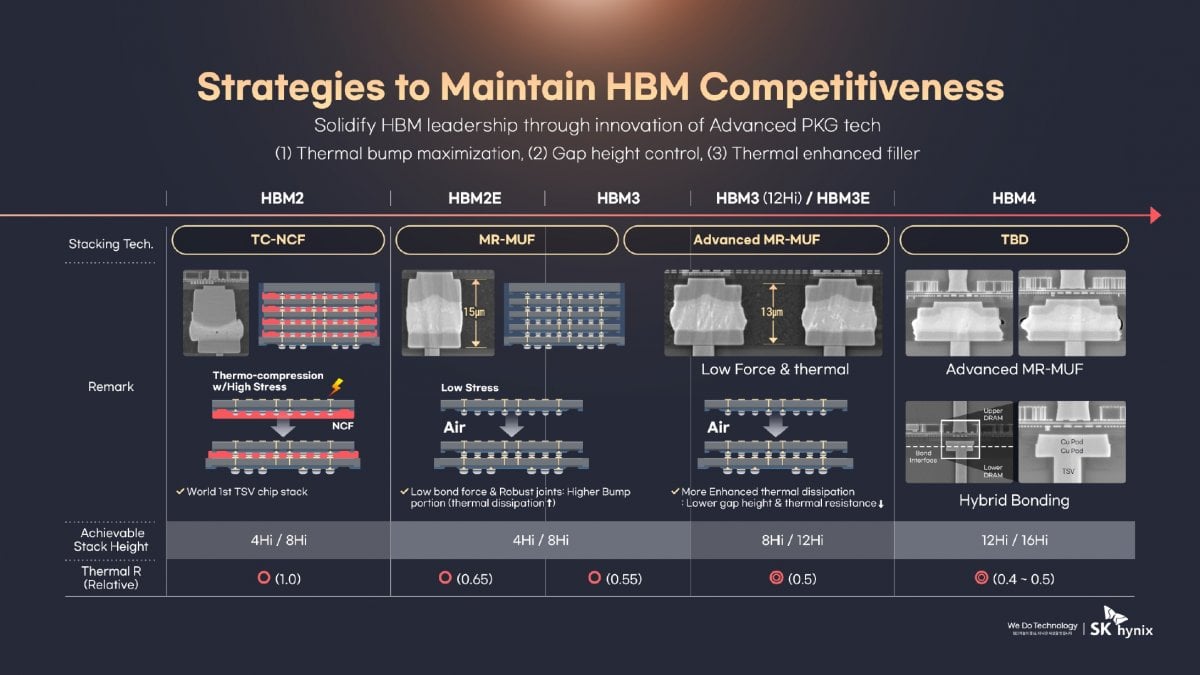
Development trend of HBM stacking technology. (Source: SK Hynix)
Advanced packaging capacity expansion and technology upgrade
In 2024, the advanced packaging market will recover, leading the packaging and testing industry to improve. In 2025, the demand for advanced packaging is expected to continue to pick up, and OSAT (packaging and testing foundry) and leading wafer fabs will further expand advanced packaging capacity and promote technology upgrades.
The development of advanced packaging technologies, such as 2.5D/3D packaging, CoWoS (Chip on Wafer on Substrate), etc., can achieve high-density integration and high-speed interconnection between chips, effectively improve system performance and reduce power consumption. With the continuous improvement of chip performance requirements in fields such as artificial intelligence, high-performance computing, and 5G communications, advanced packaging technology will become a key support for the development of the semiconductor industry, and market demand will continue to grow.
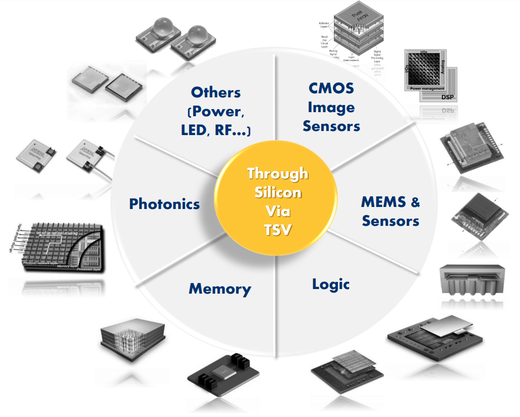
3D TSV applications are widespread and continue to grow. (Source: Yole développement)
Performance improvement and diversified development of AI processors
In 2025, a batch of new AI chips will be released or launched, with iterative updates in terms of architecture, process, and heat dissipation methods, in order to provide stronger computing power and energy efficiency, and promote the further development and application of artificial intelligence technology.
Intel will launch Panther Lake, an AI PC processor based on Intel 18A process, and Clearwater Forest, a data center processor, in 2025. Panther Lake will bring more powerful AI processing capabilities to PCs, improving user experience in image recognition, voice interaction, content creation, etc.; Clearwater Forest will be oriented to data centers to meet the needs of large-scale artificial intelligence computing and cloud computing, and improve the computing efficiency and energy utilization of data centers.
NVIDIA expects to launch the next-generation "Blackwell Ultra" GB300 in 2025, and the previously released GB200 NVL4 super chip will be available in the second half of 2025. GB300 is expected to achieve new breakthroughs in computing power and energy efficiency, continue to consolidate NVIDIA's leading position in the field of AI GPUs, and provide more powerful computing support for artificial intelligence training and reasoning. The GB200 NVL4 superchip will meet the needs of AI computing in scenarios such as data centers and edge computing with its high performance and low power consumption.
AMD will launch the next-generation AMD CDNA 4 architecture in 2025. Compared with the Instinct accelerator based on the CDNA 3 architecture, the AI reasoning performance is expected to increase by 35 times. The CDNA 4 architecture will further optimize AMD's product layout in the field of artificial intelligence, improve its competitiveness in the AI market, and provide more efficient computing solutions for applications such as deep learning and machine learning.
The continued growth in the shipment volume of AI processors will drive the development of related links such as storage and packaging, form a synergistic effect, and promote innovation and upgrading of the entire semiconductor industry chain. At the same time, with the widespread application of AI technology in various fields, higher requirements have been put forward for the performance, power consumption, and cost of AI processors, prompting chip manufacturers to continuously innovate and optimize their products.
High-end intelligent driving chip on board and technology competition
2025 is regarded by many automotive chip manufacturers as the final point of high-end intelligent driving and the window period for mass production on board. With the rapid development of automobile intelligence and electrification, the importance of high-end intelligent driving chips as core components of smart cars is becoming increasingly prominent.
In the high-end intelligent driving chip market, NVIDIA occupies an important position with its deep accumulation in the GPU field. Its Thor series and Orin-X series chips are popular in high-end smart cars. Technology giants such as Intel and Qualcomm are also not to be outdone. They have entered the market through acquisitions and other means, and market competition has become increasingly fierce. Major chip manufacturers have developed new technologies to improve chip performance to meet the growing demand for computing power. At the same time, smart driving chips are moving towards integration and are increasingly integrated with software. Chip manufacturers need to continuously optimize software algorithms and improve their intelligence level.
Quantum processor scale growth and application expansion
The United Nations announced 2025 as the "Year of Quantum Science and Technology", which shows that quantum technology has received great attention worldwide. At the end of 2024, the latest quantum processors such as Google Willow and the "Zu Chongzhi No. 3" of the University of Science and Technology of China were unveiled one after another, making breakthroughs in the number of quantum bits, quantum error correction, coherence time, and quantum computing superiority. In 2025, the industry is expected to usher in larger-scale quantum processors and computing systems.
The scale growth and performance improvement of quantum processors will promote the application expansion of quantum computing technology in scientific research, finance, cryptography, chemical simulation and other fields. In the field of scientific research, quantum computing can accelerate the progress of scientific research and help scientists solve some complex problems that are difficult to solve by traditional computers, such as protein folding and molecular simulation in materials science. In the financial field, quantum computing can be used to optimize investment portfolios, risk assessment, pricing of financial derivatives, etc., to improve the decision-making efficiency and risk management capabilities of financial institutions. In the field of cryptography, the development of quantum computing poses a challenge to traditional encryption algorithms, and also prompts scientists to study new quantum encryption algorithms to ensure information security.
Although quantum processors have made significant progress, they still face some technical challenges, such as the stability of quantum bits, the improvement of quantum error correction technology, and the scalability of quantum computing systems. In the future, we need to further increase R&D investment, break through key technical bottlenecks, and promote the maturity and widespread application of quantum processor technology.
Silicon photonic chip manufacturing technology matures
As AI servers have a sharp increase in data transmission rate requirements, silicon photonic chips that combine the advantages of silicon chip process flow and optoelectronics high speed and high energy efficiency have attracted much attention. In 2025, the manufacturing process of silicon photonic chips will mature, which will provide a more effective solution for high-speed data transmission in AI data centers.
In terms of international enterprises, NVIDIA demonstrated the silicon photonic prototype developed in cooperation with TSMC at IEDM 2024 in December 2024. TSMC will realize 1.6T optical engine for pluggable optical modules in 2025 and complete COUPE (Compact Universal Photonic Engine) verification for small pluggable products. According to TSMC, COUPE technology uses SoIC-X chip stacking technology to stack electronic dies on photonic dies, thereby providing lower resistance and higher energy efficiency at the die-to-die interface.
The maturity of silicon photonic chips will effectively solve the bandwidth bottleneck and power consumption problems of traditional electrical interconnects in high-speed data transmission, realize high-speed and low-power data transmission, and improve the overall performance and energy efficiency of data centers. With the continuous development and application of silicon photonic chip technology, it will promote innovation and development in optical communications, data centers, artificial intelligence and other fields.
SiC, Chiplet and RISC-V promote the development of automotive semiconductors
In the field of automotive semiconductors, SiC (silicon carbide), Chiplet and RISC-V technologies are becoming an important force to promote the development of the industry.
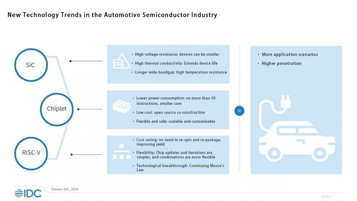
SiC power semiconductors are widely used in key components such as inverters, on-board chargers, and DC/DC converters of electric vehicles due to their advantages such as high withstand voltage, low on-resistance, and high frequency characteristics. Compared with traditional silicon-based power semiconductors, SiC devices can significantly improve the energy conversion efficiency of electric vehicles, reduce power consumption, and extend the driving range. For example, Tesla Model 3 uses SiC MOSFET in its inverter, which improves the energy efficiency of the vehicle, and has better acceleration performance and endurance performance. With the rapid growth of the electric vehicle market, the demand for SiC power semiconductors will continue to rise, promoting the continuous advancement of SiC technology and cost reduction.
Chiplet technology integrates multiple small chips (chiplets) with different functions to achieve heterogeneous integration and flexible customization of chips. In the development of high-performance automotive SoCs, chiplet technology can improve the integration and performance of chips and reduce design costs and risks. For example, by combining chiplets with different functions such as computing cores, storage units, and communication interfaces, the requirements of automotive electronic systems for high performance and multi-functions can be met. At the same time, chiplet technology can also improve the maintainability and upgradeability of chips and reduce the overall cost of the system.
RISC-V, as an open source instruction set architecture, has high flexibility and scalability, bringing new development opportunities to the automotive electronics field. The RISC-V architecture can be customized according to the specific needs of automotive electronics to achieve low-power, high-performance computing solutions. In the body control, smart cockpit, autonomous driving and other systems of automobiles, chips with RISC-V architecture can provide efficient computing support while reducing chip development costs and intellectual property risks. More and more automotive semiconductor manufacturers are beginning to pay attention to and adopt the RISC-V architecture to promote its application and development in the automotive electronics field.
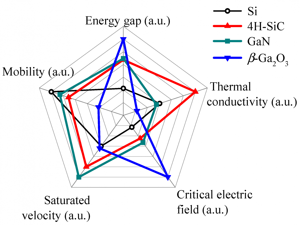
The rise of the fourth generation of semiconductor materials
The fourth generation of semiconductor materials, such as gallium oxide (Ga2O3) and aluminum nitride (AlN), are gradually becoming a research hotspot in the semiconductor field due to their unique performance advantages. Gallium oxide has the characteristics of ultra-high breakdown electric field strength, wide bandgap width and high electron mobility, which makes it have great application potential in high-voltage power devices, ultraviolet detectors and other fields. Compared with traditional silicon-based materials, gallium oxide-based power devices can operate at higher voltages and temperatures, have higher efficiency and reliability, and are expected to be used in electric vehicles, smart grids, 5G communications and other fields. Aluminum nitride has the characteristics of high thermal conductivity, high insulation and low dielectric constant, and is suitable for manufacturing high-power and high-frequency electronic devices, such as radio frequency power amplifiers and heat dissipation substrates. In 5G communication base stations, aluminum nitride heat dissipation substrates can effectively solve the heat dissipation problem of power devices and improve the performance and reliability of base stations.
Deep integration of AI and semiconductors
The deep integration of AI and semiconductors is reshaping the development pattern of the semiconductor industry. From design, manufacturing to application, AI technology has brought about all-round changes to the semiconductor industry. In the semiconductor design link, AI technology can significantly improve design efficiency and optimize chip performance. The traditional chip design process is complex and time-consuming, requiring a lot of manpower and time for verification and optimization. With the help of AI algorithms, such as machine learning and deep learning, chip design can be automatically optimized. By learning and analyzing a large amount of design data, AI can quickly find the optimal design solution, reduce the number of design iterations, and shorten the design cycle. For example, Nvidia uses AI technology to optimize the architectural design of its GPU chips, which has significantly improved the performance and energy efficiency of the chips.
In the semiconductor manufacturing process,
Impact of technology trends on the semiconductor industry
Reshaping the industry competition landscape
The mass production of 2nm and below advanced process technology will further widen the technological gap between leading companies and followers. Companies such as TSMC and Samsung, which have deep technical accumulation and huge R&D investment in the field of advanced process technology, will consolidate their dominant position in the high-end chip market with their first-mover advantage in 2nm and below processes. These companies can provide customers with higher performance and lower power consumption chip products to meet the extreme demand for chips in high-end application fields such as artificial intelligence and high-performance computing, thereby attracting more high-end customers and high-quality orders. For example, TSMC has become the main chip foundry for technology giants such as NVIDIA and Apple by virtue of its leading position in advanced process technology. The orders from these customers have brought TSMC huge profits and strong market competitiveness.
For new entrants, the ultra-high R&D costs and technical barriers of 2nm and below advanced process technology have almost become insurmountable obstacles. Building a 2nm chip production line requires tens of billions of dollars in investment and requires advanced lithography technology, precision manufacturing processes, and a strong R&D team. This makes it difficult for most new entrants to compete effectively with industry leaders in the short term.
If traditional semiconductor companies cannot keep up with the development of advanced process technology in a timely manner, they will face the risk of being marginalized by the market. In emerging fields such as artificial intelligence and 5G communications, the requirements for chip performance are constantly increasing, and only chips using advanced process technology can meet the needs of these fields. If traditional semiconductor companies still rely on mature process technology, their products will not be able to compete with chips using advanced process technology in terms of performance, power consumption, etc., resulting in a gradual erosion of market share. For example, some semiconductor companies focusing on mature process technology, in the face of the rapid rise of the artificial intelligence chip market, due to the lack of support for advanced process technology, are unable to launch products that meet market demand in a timely manner, and their market share is quickly seized by companies with advanced process technology such as Nvidia and AMD.
Driving effect on the upstream and downstream of the industrial chain
In terms of semiconductor materials, advanced process technology has put forward higher requirements on the performance of materials, which has promoted the innovation and upgrading of semiconductor materials. For example, advanced process technology of 2nm and below requires the use of silicon wafers with higher purity and lower defect density, as well as new photoresists, masks and other materials. This will prompt semiconductor material companies to increase R&D investment and improve the performance and quality of materials to meet the needs of advanced process technology. At the same time, it will also drive the development of related material equipment manufacturing companies, such as silicon wafer manufacturing equipment, photoresist coating equipment, etc.
In the field of semiconductor equipment, the development of advanced process technology has put forward higher requirements on the accuracy, efficiency and reliability of equipment. For example, extreme ultraviolet lithography (EUV) equipment is a key equipment for realizing advanced process technology of 2nm and below, and its R&D and production require extremely high technical level and manufacturing technology. The development of EUV equipment has not only driven the technological progress of lithography machine manufacturers, but also promoted the development of related supporting equipment and parts companies, such as light source systems, optical lenses, precision mechanical parts, etc. At the same time, the development of advanced packaging technology has also put forward new demands on packaging equipment, such as high-precision flip chip bonding machines, advanced 3D packaging equipment, etc., which has promoted the technological upgrading of the packaging equipment industry.
In the semiconductor design process, the deep integration of AI and semiconductors will change the traditional design process and methods. AI-assisted design tools can help designers design chip architectures, optimize circuits and verify them more efficiently, and improve design efficiency and quality. For example, through machine learning algorithms, AI can analyze and learn a large amount of design data, automatically generate optimized chip design solutions, reduce the number of design iterations, and shorten the design cycle. At the same time, AI can also be used for chip fault diagnosis and predictive maintenance to improve chip reliability and stability. This will prompt semiconductor design companies to increase the research and development and application of AI technology and enhance their own design capabilities and competitiveness.
In the semiconductor manufacturing process, the application of AI technology can realize the intelligent management and optimization of the production process. By real-time monitoring and analysis of a large amount of data on the production line, AI can promptly detect abnormal conditions in the production process and provide corresponding solutions to improve production efficiency and product yield. For example, using AI algorithms to adjust the exposure parameters of lithography machines in real time can improve lithography accuracy and reduce chip defects. At the same time, AI can also be used to optimize production scheduling, reasonably arrange the work tasks of equipment and personnel, and improve the utilization rate of production resources. This will promote semiconductor manufacturing companies to accelerate intelligent transformation and improve the automation and intelligence level of production and manufacturing.
In the field of packaging and testing, the development of advanced packaging technology will drive the innovation of packaging materials and testing equipment. For example, 2.5D/3D packaging technology requires the use of new packaging substrates, heat dissipation materials, and connection materials to achieve high-density integration and high-speed interconnection between chips. At the same time, advanced packaging technology also puts forward higher requirements on the accuracy and function of testing equipment, such as the need for equipment that can perform three-dimensional testing on chips to ensure that the performance of the packaged chips meets the requirements. This will promote packaging materials and testing equipment companies to increase R&D investment and develop new products and new technologies that meet the needs of advanced packaging technology.
Promotion of the development of emerging application fields
The progress of semiconductor technology provides strong technical support for the innovation and development of emerging fields such as artificial intelligence, the Internet of Things, and autonomous driving. In the field of artificial intelligence, the improvement and diversification of AI processor performance and the application of HBM4 technology enable artificial intelligence systems to handle more complex tasks and larger-scale data. For example, NVIDIA's A100 and H100 chips, combined with HBM high-bandwidth memory technology, provide powerful computing power for artificial intelligence training and reasoning, and promote the rapid development of artificial intelligence technologies such as deep learning, natural language processing, and computer vision. The application of these technologies has not only achieved remarkable results in the Internet field, but has also been widely used in traditional industries such as medical care, finance, and transportation, realizing intelligent upgrades.
In the field of the Internet of Things, the development of semiconductor technology enables IoT devices to achieve smaller size, lower power consumption, and higher performance. For example, microcontrollers (MCUs) and sensor chips using advanced process technology can integrate more functions and improve the intelligence level of IoT devices. At the same time, the development of wireless communication chips such as low-power Bluetooth (BLE) and ZigBee has realized efficient communication and data transmission between IoT devices. The application of these technologies has promoted the development of IoT application scenarios such as smart homes, smart industries, and smart healthcare, and realized the interconnection and intelligent management between devices.
In the field of autonomous driving, the introduction of high-end intelligent driving chips and technological competition, as well as the application of technologies such as SiC, Chiplet and RISC-V in automotive semiconductors, provide key support for the development of autonomous driving technology. For example, Nvidia's Orin series chips and Horizon's Journey series chips have powerful computing power and efficient algorithms, which can realize real-time perception, decision-making and control of the environment by autonomous driving vehicles. At the same time, the application of SiC power semiconductors improves the energy conversion efficiency and range of electric vehicles, Chiplet technology realizes heterogeneous integration and flexible customization of automotive chips, and RISC-V architecture provides low-power, high-performance computing solutions for automotive electronics. The development of these technologies has promoted the evolution of autonomous driving technology from assisted driving to fully autonomous driving, and improved driving safety and traffic efficiency.
Challenges and coping strategies faced by the semiconductor industry
Challenges and breakthrough paths in technology research and development
In terms of advanced processes, the research and development of 2nm and below processes faces many technical challenges. As the process technology continues to shrink, the density of transistors inside the chip has increased significantly, which makes the heat dissipation problem of the chip more serious. When the size of the transistor is reduced to 2nm and below, the quantum tunneling effect of electrons will become more obvious, resulting in an increase in the leakage rate of the chip, thereby affecting the performance and stability of the chip. For example, in the 2nm process, the quantum tunneling effect may cause the gate of the transistor to be unable to effectively control the flow of electrons, thereby increasing the leakage current and reducing the energy efficiency of the chip.
In order to solve these problems, enterprises and scientific research institutions are actively exploring new technologies and materials. In terms of heat dissipation, new heat dissipation materials and heat dissipation structures are developed, such as using high thermal conductivity materials as chip packaging materials, or designing more efficient heat dissipation fins and heat pipes and other heat dissipation structures to improve the heat dissipation efficiency of the chip. In terms of dealing with the quantum tunneling effect, new transistor structures and materials are studied, such as transistors with a gate-all-around (GAA) structure, which can better control the flow of electrons and reduce the impact of the quantum tunneling effect; at the same time, new semiconductor materials such as carbon nanotubes and two-dimensional materials are explored. These materials have unique electrical properties and are expected to play an important role in 2nm and below processes.
In terms of new material research and development, the research and development of fourth-generation semiconductor materials such as gallium oxide (Ga2O3) and aluminum nitride (AlN) also faces some challenges. The high-quality gallium oxide and aluminum nitride crystal growth technology is not yet fully mature, and the material defect density is high, which affects the performance and reliability of the device. At present, defects such as dislocations and impurities are prone to occur during the growth of gallium oxide crystals, which can lead to problems such as reduced breakdown voltage and increased leakage current of gallium oxide devices.
In order to break through these technical bottlenecks, scientific research institutions and enterprises have increased their R&D investment and strengthened industry-university-research cooperation. Some universities and scientific research institutions have made important progress in the basic research of new materials, such as the development of new crystal growth methods and processes that can effectively reduce the defect density of materials. Enterprises actively apply these research results to actual production, and improve the quality and performance of materials by continuously optimizing production processes and equipment. For example, by improving molecular beam epitaxy (MBE) technology and chemical vapor deposition (CVD) technology, high-quality gallium oxide and aluminum nitride crystals can be grown, laying the foundation for the industrial application of fourth-generation semiconductor materials.
Market competition and enterprise development strategy
With the intensification of competition in the semiconductor market, enterprises are facing tremendous pressure in terms of technological innovation, market expansion and cost control. In terms of technological innovation, enterprises need to continuously invest a lot of money and manpower to keep up with the pace of technological development in the industry. Developing a new chip product requires complex design, research and development, testing and other links, with a long cycle and high cost. For example, developing an advanced process AI chip may require hundreds of millions of dollars in funds and take several years.
In order to gain an advantage in technological innovation, enterprises have increased their R&D investment and established a complete R&D system. Some large semiconductor companies, such as NVIDIA and Intel, invest billions of dollars in R&D every year. At the same time, enterprises have also strengthened cooperation with universities and scientific research institutions to jointly carry out cutting-edge technology research and accelerate the process of technological innovation. For example, NVIDIA has cooperated with many universities to carry out the research and development and application research of artificial intelligence chips, which has promoted the rapid development of artificial intelligence technology.
In terms of market expansion, enterprises need to constantly look for new market opportunities and expand their market share. With the continuous emergence of emerging technologies such as artificial intelligence, the Internet of Things, and autonomous driving, the application areas of the semiconductor market are also expanding. Enterprises need to pay close attention to market trends and adjust product strategies in a timely manner to meet the needs of different markets. For example, some semiconductor companies have developed low-power, high-performance microcontrollers (MCUs) and sensor chips for the Internet of Things market to meet the demand for chips for Internet of Things devices.
In terms of cost control, enterprises need to optimize production processes and reduce production costs. Semiconductor manufacturing is a highly capital-intensive and technology-intensive industry with high production costs. Enterprises improve production efficiency and reduce production costs by adopting advanced production technologies and equipment. For example, the use of automated production equipment can reduce errors and costs caused by manual operations, improve production efficiency and product quality. At the same time, enterprises also reduce raw material procurement costs and logistics costs by optimizing supply chain management.
Talent shortage and training mechanism
The rapid development of the semiconductor industry has led to an increasing demand for talent, but the current talent shortage is quite serious. The semiconductor industry is a technology-intensive industry that requires high professional skills of talent. It takes years of professional learning and practical experience to train a qualified semiconductor engineer. Moreover, with the continuous upgrading of semiconductor technology, engineers need to constantly learn new knowledge and skills to maintain their competitiveness. This makes the training cycle of semiconductor talents longer and more difficult.
In order to strengthen talent training and attract talents, the government, universities and enterprises have taken a series of measures. The government has introduced relevant policies to increase support for semiconductor talent training. A special fund has been established to support education and research in semiconductor-related majors; universities and scientific research institutions are encouraged to strengthen the construction of semiconductor disciplines and train more professional talents. For example, the Chinese government has upgraded the integrated circuit major to a first-level discipline and increased the training of integrated circuit professionals.
Universities and scientific research institutions have also strengthened cooperation with enterprises to carry out industry-university-research cooperation projects to provide students with more practical opportunities and employment channels. Some universities have established joint laboratories with semiconductor companies to jointly carry out scientific research projects and talent training. During their studies, students can participate in the company's actual projects, accumulate practical experience, and improve their employment competitiveness.
Companies attract and retain talents by providing competitive salary packages, good career development space and training opportunities. Some companies provide employees with generous salaries, benefits and equity incentives, and also develop personalized career development plans for employees, providing training and promotion opportunities. For example, NVIDIA provides employees with broad career development space and rich training resources, attracting a large number of outstanding semiconductor talents to join.
Conclusion and Outlook
Research Summary
In 2025, the global semiconductor industry will present many remarkable technological trends, which will profoundly affect the development pattern of the industry. The mass production of 2nm and below advanced process technology will push chip performance and integration to a new height, providing stronger support for high-end applications; the breakthrough and application of HBM4 technology will greatly improve memory performance and meet the extreme demand for data processing speed in fields such as artificial intelligence; the expansion of advanced packaging capacity and technology upgrades will achieve efficient integration and interconnection of chips and promote the improvement of system performance; the improvement and diversified development of AI processor performance will accelerate the popularization and application of artificial intelligence technology; the entry and technological competition of high-end intelligent driving chips will promote the rapid development of automotive intelligence; the growth of quantum processor scale and application expansion will open a new chapter in the era of quantum computing; the maturity of silicon photonic chip manufacturing technology will solve the bottleneck problem of high-speed data transmission; the development of SiC, Chiplet and RISC-V technology will bring new changes to automotive semiconductors; the rise of the fourth-generation semiconductor materials will inject new vitality into the semiconductor industry; the deep integration of AI and semiconductors will reshape the design, manufacturing and application mode of the semiconductor industry.
These technological trends are interrelated and mutually reinforcing, and jointly promote the innovative development of the semiconductor industry. They will not only enhance the performance and competitiveness of semiconductor products, but will also provide solid technical support for the development of emerging fields such as artificial intelligence, the Internet of Things, autonomous driving, and quantum computing, and promote the rapid development and application expansion of these fields. At the same time, these technological trends will also have a profound impact on the upstream and downstream of the semiconductor industry chain, driving the technological upgrading and industrial development of various links such as semiconductor materials, equipment, design, manufacturing, packaging and testing.
Future Outlook
Looking ahead, the semiconductor industry will continue to maintain a rapid development trend, and technological innovation will become the core driving force for the development of the industry. With the continuous popularization and application of emerging technologies such as 5G, artificial intelligence, the Internet of Things, big data, and cloud computing, the demand for semiconductors will continue to grow, driving the continuous innovation and breakthroughs in the semiconductor industry. In terms of advanced process technology, we will continue to move towards smaller sizes and develop process technology of 1nm and below to further improve chip performance; in terms of storage technology, we will continue to explore new storage principles and architectures, and develop storage products with higher performance and lower power consumption; in the field of artificial intelligence chips, we will further improve the computing power and energy efficiency of chips, and develop chip architectures and algorithms that are more suitable for artificial intelligence applications; in the field of quantum computing, we will increase R&D investment, break through the bottleneck of the number and quality of quantum bits, and realize the practical application of quantum computers; in terms of semiconductor materials, we will continue to develop new materials to meet the needs of semiconductor technology development.
As the cornerstone of modern science and technology, the semiconductor industry will play an even more important role in future technological development and industrial upgrading. We look forward to more technological breakthroughs and innovative achievements in the semiconductor industry in 2025 and beyond, and to making greater contributions to the development of the global economy and the progress of human society.