Smart device interconnection solution based on NFC fast pairing of mobile phones based on ST ST25DV04K

Hedy · Dasenic Dec 09,2024 111

Smart devices and the Internet of Everything

In the smart era of the Internet of Everything, the interconnection between smart homes and mobile phones is an extremely important part. Huawei's Harmony OS system is also oriented to the Internet of Everything. Its method of connecting mobile phones with one touch requires NFC to be an indispensable function for smart devices. This article takes the blood pressure monitor in a smart device as an example to explore how the blood pressure monitor with NFC function can be used more conveniently than the traditional Bluetooth-connected blood pressure monitor, and how to quickly add NFC function to the traditional blood pressure monitor. How to do body design.


Traditional blood pressure monitor connection method

1. First open the "Sports Health" APP on your mobile phone and enter the page.

2.Find the corresponding health function on the homepage, such as "blood pressure", and click to enter.

3.Click "Measure" on the blood pressure interface to enter the binding page.

4.Select the model you purchased among the many blood pressure monitor models and click "Enter Pairing" (Bluetooth needs to be turned on).

5.Press the "Memory" button on the blood pressure monitor and click "Next" on the mobile phone interface.

6.Wait 3-5 seconds for Bluetooth pairing.


Blood pressure monitor connection method that supports NFC function

Turn on the "NFC" and "Bluetooth" functions of your phone.

Place the mobile phone's NFC antenna close to the blood pressure monitor to connect successfully.

After actual testing, the traditional method is very complicated and time-consuming. And on the model selection page, since there are many types of blood pressure monitors with similar shapes, you may choose the wrong model if you are not careful and have to go back and operate again. The blood pressure monitor equipped with NFC function is extremely convenient to pair and connect. The whole process does not require complicated operations and the connection can be completed within 3 seconds, making it more convenient for the elderly.


Introduction to NFC

Near Field Communication (NFC) is a technology used to provide short-range wireless communication for two-way interaction between electronic devices. NFC is a flavor of RFID (Radio Frequency Identification), but it also has a specific set of standards that ensure interoperability of NFC devices. The NFC standard determines the operating environment and data format, transmission rate, modulation, etc. NFC uses inductive coupling between two NFC devices and works electromagnetically, with the device operating at 13.56 MHz, an unlicensed allocation of the high-frequency portion of the radio spectrum. An NFC device can draw energy from the magnetic field generated by another NFC device. This allows some NFC devices to be powered off and take the form of tiny objects such as tags, stickers, keychains or cards.

NFC mainly has four application scenarios: mobile phones, payment, Internet, and parameter interaction. Interconnection is also a type of parameter interaction. Since the parameters of this application interaction are fixed Bluetooth or WiFi addresses, they are classified separately. The solution introduced today is to use the NFC function to quickly read the Bluetooth MAC address of the blood pressure monitor through the mobile phone to achieve quick pairing connection.


Hardware design steps for adding NFC function to traditional blood pressure monitor

Step 1. Define NFC device parameters

· Reasonable near field communication distance requirements (usually <10cm)

· Effective reader antenna size and shape

· NFC device mechanical structure (whether there is metal shielding near the card reader or tag antenna, such as PCB copper coating, lithium battery, metal casing, etc.)

· Type of label (ISO15693, ISO14443)

· Card reader performance (mobile phone or card reader? Card reader antenna shape, size, transmission power, etc.)

· Other requirements (such as energy transmission function, multi-card operation, etc.)

Step 2. Use a reader (ST25R3916-DISCO or ST25R3911B-DISCO) or an NFC mobile phone to evaluate the communication distance of NFC tags with different antenna sizes and build a product prototype.

Step 3. Determine tag antenna size and design antenna (AN2866)
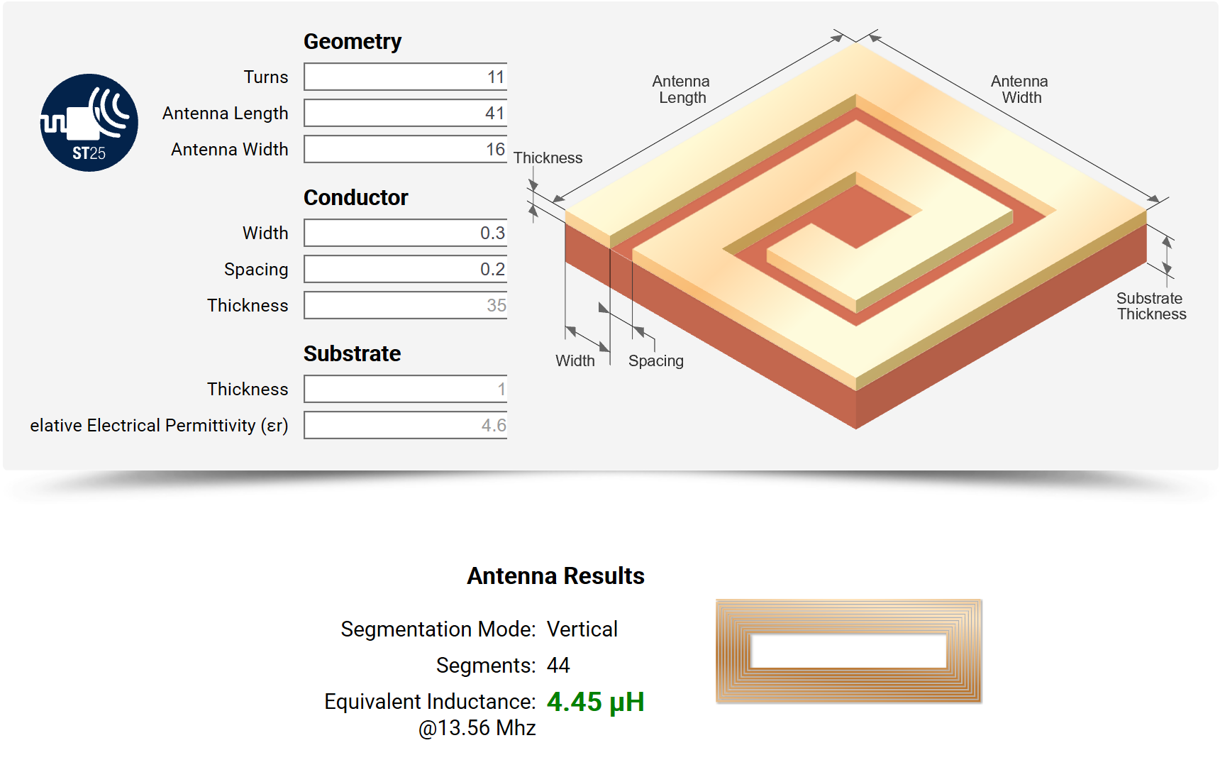
Step 4. For schematic diagram and PCB layout design, please refer to ST25D series Nucleo board schematic diagram and PCB layout.

Step 5. According to the design requirements of the tag antenna inductance L, process 3 tag PCB styles within the range of the antenna inductance L +/-300nH (antenna target inductance: L-300nH,

L, L+300nH).

The inductance L of ST25DV04K is required to be 4.6uH.

Step 6. Measure and test the tag antenna, fine-tune the antenna impedance matching or optimize the antenna design (if necessary), and determine the optimal design:

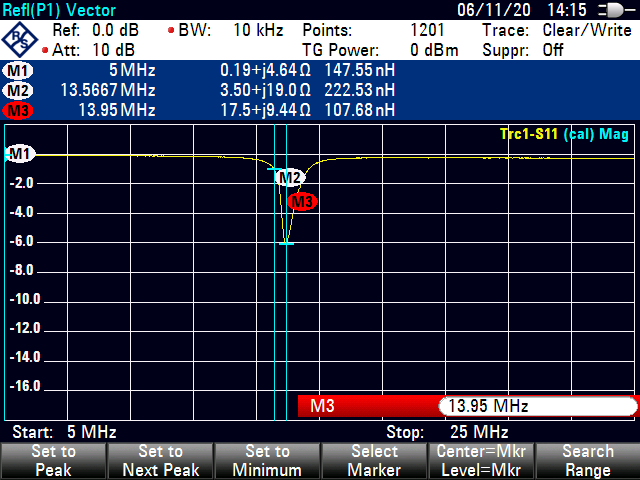
The resonance of the antenna designed and produced according to step 3 is as shown below:

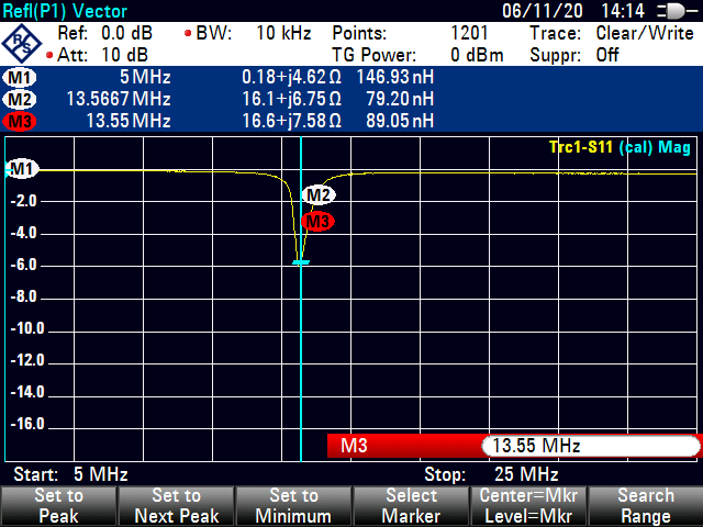
The resonant frequency of the antenna after fine-tuning the parallel 2pf capacitor is as shown below:

The test results are as follows:

Distance test with ST25R3916 discovery Demo boardOriginalHuawei P30
ST25R3916 discovery Demo9cm9cm
Huawei P303.5cm3.5cm

Due to the better initial antenna design, the card reading distance has not been significantly improved after fine-tuning. If the size of the antenna is small or there is metal influence around it, the resonant frequency of the designed tag antenna may deviate greatly, seriously affecting the card reading performance. At this time, you need to adjust the impedance matching and adjust the resonant frequency back to around 13.56Mhz to optimize card reading performance.

Step 7. System integration, MCU firmware development (I2C communication, such as dynamic tag ST25DV/M24SR)

ST provides mobile phone apk file source code based on STM32Cube and ST official demo.

ST25DV communicates with the MCU through I2C, and can change the data read by the NFC of the mobile phone at any time when the power is supplied, and is not limited to the MAC address.

On the mobile phone APP side, traditional smart device manufacturers already have APPs for use with their devices. They only need to make a small upgrade to the original APP to receive the NDEF data read from NFC.

To sum up, to add NFC function to traditional smart devices, customers need to add ST25DV and antenna to the original PCB in hardware, integrate the ST25DV driver in MCU software, and make a small upgrade on the APP.


Scenario application diagram
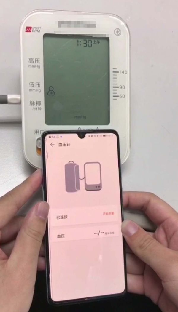
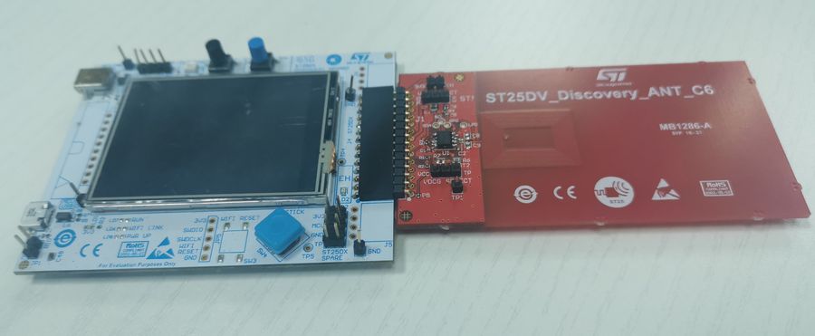
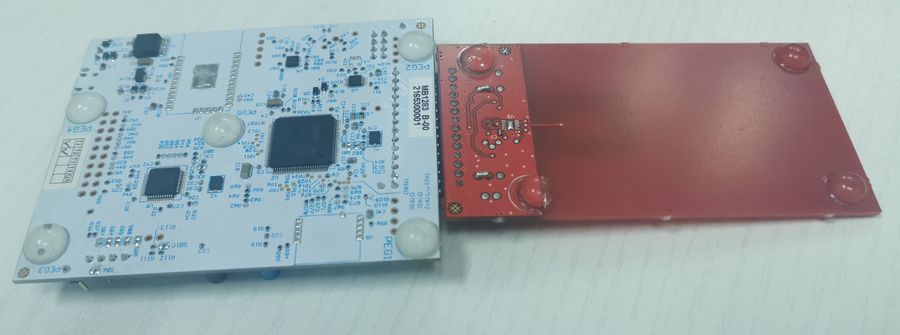
Product entity diagram

Display board photo

Solution block diagram
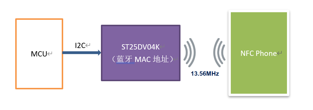
Antenna design

Core technical advantages

The ST25DV04K, ST25DV16K and ST25DV64K devices are NFC RFID tags offering 4 Kbit, 16 Kbit and 64 Kbit electrically erasable programmable memory (EEPROM) respectively. ST25DV04K, ST25DV16K and ST25DV64K provide two interfaces. The first is an I2C serial connection that can run from DC power. The second is the RF link that is activated when the ST25DV04K, ST25DV16K or ST25DV64K acts as a contactless memory driven by a received carrier electromagnetic wave.

In I2C mode, the user memory of ST25DV04K, ST25DV16K and ST25DV64K is up to 512 bytes, 2048 bytes and 8192 bytes, which can be divided into 4 flexible protectable areas.

In RF mode, the ST25DV04K, ST25DV16K and ST25DV64K user memories contain up to 128 blocks, 512 blocks and 2048 blocks of 4 bytes respectively, which can be split into 4 Flexible, protectable areas.


Solution specifications

I2C interface

Two-wire I2C serial interface supports 1MHz protocol

Single power supply voltage: 1.8V ~ 5.5V

Multi-byte programming (up to 256 bytes)


Contactless interface

According to ISO/IEC 15693

NFC Forum Type 5 tag certified by NFC Forum

Supports all ISO/IEC 15693 modulations, encodings, subcarrier modes and data rates

Customizable fast read access up to 53 Kbit/s

Read single and multiple blocks (same goes for extended commands)

Single and multi-block writes (up to 4) (same goes for extended commands)

Internal tuning capacitor: 28.5 pF


Memory

Up to 64 kbits of EEPROM (depending on version)

I2C interface access byte

RF interface accesses 4-byte blocks

Writing time:

From I2C: typical 1 byte 5ms

From RF: Typical 5 ms for 1 block

Data retention: 40 years

Write cycle endurance:

1 million write cycles at 25°C

Write 600k cycles at 85℃

500k write cycle at 105℃

400,000 write cycles at 125°C


Fast transfer mode

Fast data transfer between I2C and RF interface

Half-duplex 256-byte dedicated buffer


Energy Harvesting: Analog Output Pins Power External Components


Data protection

User memory: 1 to 4 configurable areas, read and write protected with 3 64-bit RF passwords and 1 64-bit I2C password

System Configuration: The write protection consists of a 64-bit password in RF and a 64-bit password in I2C


GPO

Configurable interrupt pins on multiple RF events (field change, memory write, activity, fast transfer, user set/reset/pulse)

Open drain or CMOS output (depending on version)


Low power mode (10-ball 12-pin package only)

Input pin triggers low power mode


RF management

RF command interpreter enable/disable from I2C host controller


Temperature range

Range 6: from -40 to 85 degrees Celsius

Range 8: from -40 to 105 degrees Celsius

(Applies to UDFPN8 and UDFPN12 only)

-40 ~ 125℃ (only applicable to SO8N and TSSOP8, RF interface maximum 105℃)


Package

8-pin, 10-ball and 12-pin packages

ECOPACK2® (lead-free certified)


Order the same NFC Discovery Kit

ST25R3916-DISCO

ST25R3911B-DISCO


Smart device interconnection solution based on NFC fast pairing of mobile phones based on ST ST25DV04K

Hedy · Dasenic Dec 09,2024 111

Smart devices and the Internet of Everything

In the smart era of the Internet of Everything, the interconnection between smart homes and mobile phones is an extremely important part. Huawei's Harmony OS system is also oriented to the Internet of Everything. Its method of connecting mobile phones with one touch requires NFC to be an indispensable function for smart devices. This article takes the blood pressure monitor in a smart device as an example to explore how the blood pressure monitor with NFC function can be used more conveniently than the traditional Bluetooth-connected blood pressure monitor, and how to quickly add NFC function to the traditional blood pressure monitor. How to do body design.


Traditional blood pressure monitor connection method

1. First open the "Sports Health" APP on your mobile phone and enter the page.

2.Find the corresponding health function on the homepage, such as "blood pressure", and click to enter.

3.Click "Measure" on the blood pressure interface to enter the binding page.

4.Select the model you purchased among the many blood pressure monitor models and click "Enter Pairing" (Bluetooth needs to be turned on).

5.Press the "Memory" button on the blood pressure monitor and click "Next" on the mobile phone interface.

6.Wait 3-5 seconds for Bluetooth pairing.


Blood pressure monitor connection method that supports NFC function

Turn on the "NFC" and "Bluetooth" functions of your phone.

Place the mobile phone's NFC antenna close to the blood pressure monitor to connect successfully.

After actual testing, the traditional method is very complicated and time-consuming. And on the model selection page, since there are many types of blood pressure monitors with similar shapes, you may choose the wrong model if you are not careful and have to go back and operate again. The blood pressure monitor equipped with NFC function is extremely convenient to pair and connect. The whole process does not require complicated operations and the connection can be completed within 3 seconds, making it more convenient for the elderly.


Introduction to NFC

Near Field Communication (NFC) is a technology used to provide short-range wireless communication for two-way interaction between electronic devices. NFC is a flavor of RFID (Radio Frequency Identification), but it also has a specific set of standards that ensure interoperability of NFC devices. The NFC standard determines the operating environment and data format, transmission rate, modulation, etc. NFC uses inductive coupling between two NFC devices and works electromagnetically, with the device operating at 13.56 MHz, an unlicensed allocation of the high-frequency portion of the radio spectrum. An NFC device can draw energy from the magnetic field generated by another NFC device. This allows some NFC devices to be powered off and take the form of tiny objects such as tags, stickers, keychains or cards.

NFC mainly has four application scenarios: mobile phones, payment, Internet, and parameter interaction. Interconnection is also a type of parameter interaction. Since the parameters of this application interaction are fixed Bluetooth or WiFi addresses, they are classified separately. The solution introduced today is to use the NFC function to quickly read the Bluetooth MAC address of the blood pressure monitor through the mobile phone to achieve quick pairing connection.


Hardware design steps for adding NFC function to traditional blood pressure monitor

Step 1. Define NFC device parameters

· Reasonable near field communication distance requirements (usually <10cm)

· Effective reader antenna size and shape

· NFC device mechanical structure (whether there is metal shielding near the card reader or tag antenna, such as PCB copper coating, lithium battery, metal casing, etc.)

· Type of label (ISO15693, ISO14443)

· Card reader performance (mobile phone or card reader? Card reader antenna shape, size, transmission power, etc.)

· Other requirements (such as energy transmission function, multi-card operation, etc.)

Step 2. Use a reader (ST25R3916-DISCO or ST25R3911B-DISCO) or an NFC mobile phone to evaluate the communication distance of NFC tags with different antenna sizes and build a product prototype.

Step 3. Determine tag antenna size and design antenna (AN2866)

Step 4. For schematic diagram and PCB layout design, please refer to ST25D series Nucleo board schematic diagram and PCB layout.

Step 5. According to the design requirements of the tag antenna inductance L, process 3 tag PCB styles within the range of the antenna inductance L +/-300nH (antenna target inductance: L-300nH,

L, L+300nH).

The inductance L of ST25DV04K is required to be 4.6uH.

Step 6. Measure and test the tag antenna, fine-tune the antenna impedance matching or optimize the antenna design (if necessary), and determine the optimal design:

The resonance of the antenna designed and produced according to step 3 is as shown below:


The resonant frequency of the antenna after fine-tuning the parallel 2pf capacitor is as shown below:


The test results are as follows:

Distance test with ST25R3916 discovery Demo boardOriginalHuawei P30
ST25R3916 discovery Demo9cm9cm
Huawei P303.5cm3.5cm

Due to the better initial antenna design, the card reading distance has not been significantly improved after fine-tuning. If the size of the antenna is small or there is metal influence around it, the resonant frequency of the designed tag antenna may deviate greatly, seriously affecting the card reading performance. At this time, you need to adjust the impedance matching and adjust the resonant frequency back to around 13.56Mhz to optimize card reading performance.

Step 7. System integration, MCU firmware development (I2C communication, such as dynamic tag ST25DV/M24SR)

ST provides mobile phone apk file source code based on STM32Cube and ST official demo.

ST25DV communicates with the MCU through I2C, and can change the data read by the NFC of the mobile phone at any time when the power is supplied, and is not limited to the MAC address.

On the mobile phone APP side, traditional smart device manufacturers already have APPs for use with their devices. They only need to make a small upgrade to the original APP to receive the NDEF data read from NFC.

To sum up, to add NFC function to traditional smart devices, customers need to add ST25DV and antenna to the original PCB in hardware, integrate the ST25DV driver in MCU software, and make a small upgrade on the APP.


Scenario application diagram

Product entity diagram

Display board photo

Solution block diagram

Antenna design

Core technical advantages

The ST25DV04K, ST25DV16K and ST25DV64K devices are NFC RFID tags offering 4 Kbit, 16 Kbit and 64 Kbit electrically erasable programmable memory (EEPROM) respectively. ST25DV04K, ST25DV16K and ST25DV64K provide two interfaces. The first is an I2C serial connection that can run from DC power. The second is the RF link that is activated when the ST25DV04K, ST25DV16K or ST25DV64K acts as a contactless memory driven by a received carrier electromagnetic wave.

In I2C mode, the user memory of ST25DV04K, ST25DV16K and ST25DV64K is up to 512 bytes, 2048 bytes and 8192 bytes, which can be divided into 4 flexible protectable areas.

In RF mode, the ST25DV04K, ST25DV16K and ST25DV64K user memories contain up to 128 blocks, 512 blocks and 2048 blocks of 4 bytes respectively, which can be split into 4 Flexible, protectable areas.


Solution specifications

I2C interface

Two-wire I2C serial interface supports 1MHz protocol

Single power supply voltage: 1.8V ~ 5.5V

Multi-byte programming (up to 256 bytes)


Contactless interface

According to ISO/IEC 15693

NFC Forum Type 5 tag certified by NFC Forum

Supports all ISO/IEC 15693 modulations, encodings, subcarrier modes and data rates

Customizable fast read access up to 53 Kbit/s

Read single and multiple blocks (same goes for extended commands)

Single and multi-block writes (up to 4) (same goes for extended commands)

Internal tuning capacitor: 28.5 pF


Memory

Up to 64 kbits of EEPROM (depending on version)

I2C interface access byte

RF interface accesses 4-byte blocks

Writing time:

From I2C: typical 1 byte 5ms

From RF: Typical 5 ms for 1 block

Data retention: 40 years

Write cycle endurance:

1 million write cycles at 25°C

Write 600k cycles at 85℃

500k write cycle at 105℃

400,000 write cycles at 125°C


Fast transfer mode

Fast data transfer between I2C and RF interface

Half-duplex 256-byte dedicated buffer


Energy Harvesting: Analog Output Pins Power External Components


Data protection

User memory: 1 to 4 configurable areas, read and write protected with 3 64-bit RF passwords and 1 64-bit I2C password

System Configuration: The write protection consists of a 64-bit password in RF and a 64-bit password in I2C


GPO

Configurable interrupt pins on multiple RF events (field change, memory write, activity, fast transfer, user set/reset/pulse)

Open drain or CMOS output (depending on version)


Low power mode (10-ball 12-pin package only)

Input pin triggers low power mode


RF management

RF command interpreter enable/disable from I2C host controller


Temperature range

Range 6: from -40 to 85 degrees Celsius

Range 8: from -40 to 105 degrees Celsius

(Applies to UDFPN8 and UDFPN12 only)

-40 ~ 125℃ (only applicable to SO8N and TSSOP8, RF interface maximum 105℃)


Package

8-pin, 10-ball and 12-pin packages

ECOPACK2® (lead-free certified)


Order the same NFC Discovery Kit

ST25R3916-DISCO

ST25R3911B-DISCO


  • RFQ